
The chip made for the AI inference era – the Google TPU

Hey everyone,
As I find the topic of Google TPUs extremely important, I am publishing a comprehensive deep dive, not just a technical overview, but also strategic and financial coverage of the Google TPU.
Topics covered:
The history of the TPU and why it all even started?
The difference between a TPU and a GPU?
Performance numbers TPU vs GPU?
Where are the problems for the wider adoption of TPUs
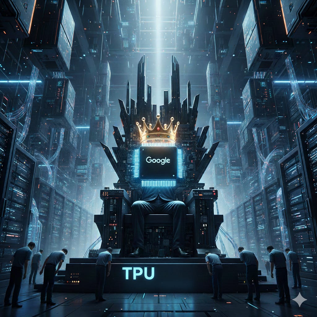
Google’s TPU is the biggest competitive advantage of its cloud business for the next 10 years
How many TPUs does Google produce today, and how big can that get?
Gemini 3 and the aftermath of Gemini 3 on the whole chip industry
Let’s dive into it.
The history of the TPU and why it all even started?
The story of the Google Tensor Processing Unit (TPU) begins not with a breakthrough in chip manufacturing, but with a realization about math and logistics. Around 2013, Google’s leadership—specifically Jeff Dean, Jonathan Ross (the CEO of Groq), and the Google Brain team—ran a projection that alarmed them. They calculated that if every Android user utilized Google’s new voice search feature for just three minutes a day, the company would need to double its global data center capacity just to handle the compute load.
At the time, Google was relying on standard CPUs and GPUs for these tasks. While powerful, these general-purpose chips were inefficient for the specific heavy lifting required by Deep Learning: massive matrix multiplications. Scaling up with existing hardware would have been a financial and logistical nightmare.
This sparked a new project. Google decided to do something rare for a software company: build its own custom silicon. The goal was to create an ASIC (Application-Specific Integrated Circuit) designed for one job only: running TensorFlow neural networks.
Key Historical Milestones:
2013-2014: The project moved really fast as Google both hired a very capable team and, to be honest, had some luck in their first steps. The team went from design concept to deploying silicon in data centers in just 15 months—a very short cycle for hardware engineering.
2015: Before the world knew they existed, TPUs were already powering Google’s most popular products. They were silently accelerating Google Maps navigation, Google Photos, and Google Translate.
2016: Google officially unveiled the TPU at Google I/O 2016.
This urgency to solve the “data center doubling” problem is why the TPU exists. It wasn’t built to sell to gamers or render video; it was built to save Google from its own AI success. With that in mind, Google has been thinking about the »costly« AI inference problems for over a decade now. This is also one of the main reasons why the TPU is so good today compared to other ASIC projects.
The difference between a TPU and a GPU?
To understand the difference, it helps to look at what each chip was originally built to do. A GPU is a “general-purpose” parallel processor, while a TPU is a “domain-specific” architecture.
The GPUs were designed for graphics. They excel at parallel processing (doing many things at once), which is great for AI. However, because they are designed to handle everything from video game textures to scientific simulations, they carry “architectural baggage.” They spend significant energy and chip area on complex tasks like caching, branch prediction, and managing independent threads.
A TPU, on the other hand, strips away all that baggage. It has no hardware for rasterization or texture mapping. Instead, it uses a unique architecture called a Systolic Array.
The “Systolic Array” is the key differentiator. In a standard CPU or GPU, the chip moves data back and forth between the memory and the computing units for every calculation. This constant shuffling creates a bottleneck (the Von Neumann bottleneck).
In a TPU’s systolic array, data flows through the chip like blood through a heart (hence “systolic”).
It loads data (weights) once.
It passes inputs through a massive grid of multipliers.
The data is passed directly to the next unit in the array without writing back to memory.
What this means, in essence, is that a TPU, because of its systolic array, drastically reduces the number of memory reads and writes required from HBM. As a result, the TPU can spend its cycles computing rather than waiting for data.
Google’s new TPU design, also called Ironwood also addressed some of the key areas where a TPU was lacking:
They enhanced the SparseCore for efficiently handling large embeddings (good for recommendation systems and LLMs)
It increased HBM capacity and bandwidth (up to 192 GB per chip). For a better understanding, Nvidia’s Blackwell B200 has 192GB per chip, while Blackwell Ultra, also known as the B300, has 288 GB per chip.
Improved the Inter-Chip Interconnect (ICI) for linking thousands of chips into massive clusters, also called TPU Pods (needed for AI training as well as some time test compute inference workloads). When it comes to ICI, it is important to note that it is very performant with a Peak Bandwidth of 1.2 TB/s vs Blackwell NVLink 5 at 1.8 TB/s. But Google’s ICI, together with its specialized compiler and software stack, still delivers superior performance on some specific AI tasks.
The key thing to understand is that because the TPU doesn’t need to decode complex instructions or constantly access memory, it can deliver significantly higher Operations Per Joule.
For scale-out, Google uses Optical Circuit Switch (OCS) and its 3D torus network, which compete with Nvidia’s InfiniBand and Spectrum-X Ethernet. The main difference is that OCS is extremely cost-effective and power-efficient as it eliminates electrical switches and O-E-O conversions, but because of this, it is not as flexible as the other two. So again, the Google stack is extremely specialized for the task at hand and doesn’t offer the flexibility that GPUs do.
Performance numbers TPU vs GPU?
As we defined the differences, let’s look at real numbers showing how the TPU performs compared to the GPU. Since Google isn’t revealing these numbers, it is really hard to get details on performance. I studied many articles and alternative data sources, including interviews with industry insiders, and here are some of the key takeaways.
The first important thing is that there is very limited information on Google’s newest TPUv7 (Ironwood), as Google introduced it in April 2025 and is just now starting to become available to external clients (internally, it is said that Google has already been using Ironwood since April, possibly even for Gemini 3.0.). And why is this important if we, for example, compare TPUv7 with an older but still widely used version of TPUv5p based on Semianalysis data:
TPUv7 produces 4,614 TFLOPS(BF16) vs 459 TFLOPS for TPUv5p
TPUv7 has 192GB of memory capacity vs TPUv5p 96GB
TPUv7 memory Bandwidth is 7,370 GB/s vs 2,765 for v5p
We can see that the performance leaps between v5 and v7 are very significant. To put that in context, most of the comments that we will look at are more focused on TPUv6 or TPUv5 than v7.
Based on analyzing a ton of interviews with Former Google employees, customers, and competitors (people from AMD, NVDA & others), the summary of the results is as follows.
Most agree that TPUs are more cost-effective compared to Nvidia GPUs, and most agree that the performance per watt for TPUs is better. This view is not applicable across all use cases tho.
A Former Google Cloud employee:
»If it is the right application, then they can deliver much better performance per dollar compared to GPUs. They also require much lesser energy and produces less heat compared to GPUs. They’re also more energy efficient and have a smaller environmental footprint, which is what makes them a desired outcome.
The use cases are slightly limited to a GPU, they’re not as generic, but for a specific application, they can offer as much as 1.4X better performance per dollar, which is pretty significant saving for a customer that might be trying to use GPU versus TPUs.«
source: AlphaSense
Similarly, a very insightful comment from a Former Unit Head at Google around TPUs materially lowering AI-search cost per query vs GPUs:
»TPU v6 is 60-65% more efficient than GPUs, prior generations 40-45%«
This interview was in November 2024, so the expert is probably comparing the v6 TPU with the Nvidia Hopper. Today, we already have Blackwell vs V7.
Many experts also mention the speed benefit that TPUs offer, with a Former Google Head saying that TPUs are 5x faster than GPUs for training dynamic models (like search-like workloads).
There was also a very eye-opening interview with a client who used both Nvidia GPUs and Google TPUs as he describes the economics in great detail:
»If I were to use eight H100s versus using one v5e pod, I would spend a lot less money on one v5e pod. In terms of price point money, performance per dollar, you will get more bang for TPU. If I already have a code, because of Google’s help or because of our own work, if I know it already is going to work on a TPU, then at that point it is beneficial for me to just stick with the TPU usage.
In the long run, if I am thinking I need to write a new code base, I need to do a lot more work, then it depends on how long I’m going to train. I would say there is still some, for example, of the workload we have already done on TPUs that in the future because as Google will add newer generation of TPU, they make older ones much cheaper.
For example, when they came out with v4, I remember the price of v2 came down so low that it was practically free to use compared to any NVIDIA GPUs.
Google has got a good promise so they keep supporting older TPUs and they’re making it a lot cheaper. If you don’t really need your model trained right away, if you’re willing to say, “I can wait one week,” even though the training is only three days, then you can reduce your cost 1/5.«
source: AlphaSense
Another valuable interview was with a current AMD employee, acknowledging the benefits of ASICs:
»I would expect that an AI accelerator could do about probably typically what we see in the industry. I’m using my experience at FPGAs. I could see a 30% reduction in size and maybe a 50% reduction in power vs a GPU.«
We also got some numbers from a Former Google employee who worked in the chip segment:
»When I look at the published numbers, they (TPUs) are anywhere from 25%-30% better to close to 2x better, depending on the use cases compared to Nvidia. Essentially, there’s a difference between a very custom design built to do one task perfectly versus a more general purpose design.«
What is also known is that the real edge of TPUs lies not in the hardware but in the software and in the way Google has optimized its ecosystem for the TPU.
A lot of people mention the problem that every Nvidia »competitor« like the TPU faces, which is the fast development of Nvidia and the constant »catching up« to Nvidia problem. This month a former Google Cloud employee addressed that concern head-on as he believes the rate at which TPUs are improving is faster than the rate at Nvidia:
»The amount of performance per dollar that a TPU can generate from a new generation versus the old generation is a much significant jump than Nvidia«
In addition, the recent data from Google’s presentation at the Hot Chips 2025 event backs that up, as Google stated that the TPUv7 is 100% better in performance per watt than their TPUv6e (Trillium).
Even for hard Nvidia advocates, TPUs are not to be shrugged off easily, as even Jensen thinks very highly of Google’s TPUs. In a podcast with Brad Gerstner, he mentioned that when it comes to ASICs, Google with TPUs is a »special case«. A few months ago, we also got an article from the WSJ saying that after the news publication The Information published a report that stated that OpenAI had begun renting Google TPUs for ChatGPT, Jensen called Altman, asking him if it was true, and signaled that he was open to getting the talks back on track (investment talks). Also worth noting was that Nvidia’s official X account posted a screenshot of an article in which OpenAI denied plans to use Google’s in-house chips. To say the least, Nvidia is watching TPUs very closely.
Ok, but after looking at some of these numbers, one might think, why aren’t more clients using TPUs?
Where are the problems for the wider adoption of TPUs
The main problem for TPUs adoption is the ecosystem. Nvidia’s CUDA is engraved in the minds of most AI engineers, as they have been learning CUDA in universities. Google has developed its ecosystem internally but not externally, as it has used TPUs only for its internal workloads until now. TPUs use a combination of JAX and TensorFlow, while the industry skews to CUDA and PyTorch (although TPUs also support PyTorch now). While Google is working hard to make its ecosystem more supportive and convertible with other stacks, it is also a matter of libraries and ecosystem formation that takes years to develop.
It is also important to note that, until recently, the GenAI industry’s focus has largely been on training workloads. In training workloads, CUDA is very important, but when it comes to inference, even reasoning inference, CUDA is not that important, so the chances of expanding the TPU footprint in inference are much higher than those in training (although TPUs do really well in training as well – Gemini 3 the prime example).
The fact that most clients are multi-cloud also poses a challenge for TPU adoption, as AI workloads are closely tied to data and its location (cloud data transfer is costly). Nvidia is accessible via all three hyperscalers, while TPUs are available only at GCP so far. A client who uses TPUs and Nvidia GPUs explains it well:
»Right now, the one biggest advantage of NVIDIA, and this has been true for past three companies I worked on is because AWS, Google Cloud and Microsoft Azure, these are the three major cloud companies.
Every company, every corporate, every customer we have will have data in one of these three. All these three clouds have NVIDIA GPUs. Sometimes the data is so big and in a different cloud that it is a lot cheaper to run our workload in whatever cloud the customer has data in.
I don’t know if you know about the egress cost that is moving data out of one cloud is one of the bigger cost. In that case, if you have NVIDIA workload, if you have a CUDA workload, we can just go to Microsoft Azure, get a VM that has NVIDIA GPU, same GPU in fact, no code change is required and just run it there.
With TPUs, once you are all relied on TPU and Google says, “You know what? Now you have to pay 10X more,” then we would be screwed, because then we’ll have to go back and rewrite everything. That’s why. That’s the only reason people are afraid of committing too much on TPUs. The same reason is for Amazon’s Trainium and Inferentia.«
source: AlphaSense
These problems are well known at Google, so it is no surprise that internally, the debate over keeping TPUs inside Google or starting to sell them externally is a constant topic. When keeping them internally, it enhances the GCP moat, but at the same time, many former Google employees believe that at some point, Google will start offering TPUs externally as well, maybe through some neoclouds, not necessarily with the biggest two competitors, Microsoft and Amazon. Opening up the ecosystem, providing support, etc., and making it more widely usable are the first steps toward making that possible.
A former Google employee also mentioned that Google last year formed a more sales-oriented team to push and sell TPUs, so it’s not like they have been pushing hard to sell TPUs for years; it is a fairly new dynamic in the organization.
Google’s TPU is the biggest competitive advantage of its cloud business for the next 10 years
The most valuable thing for me about TPUs is their impact on GCP. As we witness the transformation of cloud businesses from the pre-AI era to the AI era, the biggest takeaway is that the industry has gone from an oligopoly of AWS, Azure, and GCP to a more commoditized landscape, with Oracle, Coreweave, and many other neoclouds competing for AI workloads. The problem with AI workloads is the competition and Nvidia’s 75% gross margin, which also results in low margins for AI workloads. The cloud industry is moving from a 50-70% gross margin industry to a 20-35% gross margin industry. For cloud investors, this should be concerning, as the future profile of some of these companies is more like that of a utility than an attractive, high-margin business. But there is a solution to avoiding that future and returning to a normal margin: the ASIC.
The cloud providers who can control the hardware and are not beholden to Nvidia and its 75% gross margin will be able to return to the world of 50% gross margins. And there is no surprise that all three AWS, Azure, and GCP are developing their own ASICs. The most mature by far is Google’s TPU, followed by Amazon’s Trainum, and lastly Microsoft’s MAIA (although Microsoft owns the full IP of OpenAI’s custom ASICs, which could help them in the future).
While even with ASICs you are not 100% independent, as you still have to work with someone like Broadcom or Marvell, whose margins are lower than Nvidia’s but still not negligible, Google is again in a very good position. Over the years of developing TPUs, Google has managed to control much of the chip design process in-house. According to a current AMD employee, Broadcom no longer knows everything about the chip. At this point, Google is the front-end designer (the actual RTL of the design) while Broadcom is only the backend physical design partner. Google, on top of that, also, of course, owns the entire software optimization stack for the chip, which makes it as performant as it is. According to the AMD employee, based on this work split, he thinks Broadcom is lucky if it gets a 50-point gross margin on its part.
Without having to pay Nvidia for the accelerator, a cloud provider can either price its compute similarly to others and maintain a better margin profile or lower costs and gain market share. Of course, all of this depends on having a very capable ASIC that can compete with Nvidia. Unfortunately, it looks like Google is the only one that has achieved that, as the number one-performing model is Gemini 3 trained on TPUs. According to some former Google employees, internally, Google is also using TPUs for inference across its entire AI stack, including Gemini and models like Veo. Google buys Nvidia GPUs for GCP, as clients want them because they are familiar with them and the ecosystem, but internally, Google is full-on with TPUs.
As the complexity of each generation of ASICs increases, similar to the complexity and pace of Nvidia, I predict that not all ASIC programs will make it. I believe outside of TPUs, the only real hyperscaler shot right now is AWS Trainium, but even that faces much bigger uncertainties than the TPU. With that in mind, Google and its cloud business can come out of this AI era as a major beneficiary and market-share gainer.
Recently, we even got comments from the SemiAnalysis team praising the TPU:
»Google’s silicon supremacy among hyperscalers is unmatched, with their TPU 7th Gen arguably on par with Nvidia Blackwell. TPU powers the Gemini family of models which are improving in capability and sit close to the pareto frontier of $ per intelligence in some tasks«
source: SemiAnalysis
How many TPUs does Google produce today, and how big can that get?
Here are the numbers that I researched: